카지노사이트의 쿠폰, 이벤트, 프로모션, 보증
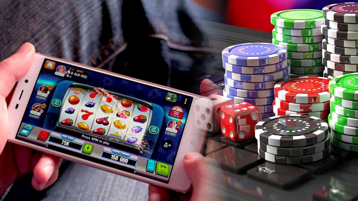
카지노사이트는 현대 사회에서 많은 이들에게 인기를 끌고 있는 온라인 엔터테인먼트 플랫폼 중 하나입니다. 카지노사이트에서는 다양한 게임을 즐길 수 있으며, 놀라운 쿠폰, 흥미로운 이벤트, 유혹적인 프로모션, 그리고 안정적인보증까지 제공되어 사용자들의 많은 호응을 얻고 있습니다. 가장 큰 매력 중 하나는 바로 다양한 쿠폰과 이벤트입니다. 이를 통해 사용자들은 게임을 즐기면서 추가 혜택을 받을...

카지노사이트는 현대 사회에서 많은 이들에게 인기를 끌고 있는 온라인 엔터테인먼트 플랫폼 중 하나입니다. 카지노사이트에서는 다양한 게임을 즐길 수 있으며, 놀라운 쿠폰, 흥미로운 이벤트, 유혹적인 프로모션, 그리고 안정적인보증까지 제공되어 사용자들의 많은 호응을 얻고 있습니다. 가장 큰 매력 중 하나는 바로 다양한 쿠폰과 이벤트입니다. 이를 통해 사용자들은 게임을 즐기면서 추가 혜택을 받을...

온라인바카라는 전 세계적으로 인기 있는 카지노 게임 중 하나로, 많은 이용자들이 즐기고 있습니다. 이 게임은 2장의 카드를 이용하여 가까운 수를 가진 쪽이 이기는 간단한 룰로 쉽게 즐길 수 있습니다. 온라인바카라의 매력 온라인바카라는 직접 카지노에 방문하지 않아도 가장 현실감 있는 경험을 제공해줍니다. 예전에는 온라인바카라 벽에만 붙어 있던 바카라가 이제 온라인으로 얼마든지...

마사지 커뮤니티란 무엇인가? 마사지 커뮤니티는 다양한 마사지 정보와 리뷰를 공유하는 온라인 공간으로, 마사지를 사랑하는 사람들이 진정한 휴식과 치유를 찾아 서로의 경험을 나누는 곳입니다. 이곳에서는 전문가의 손길을 거쳐 정제된 정보만을 만나볼 수 있으며, 사용자들은 실시간으로 서비스에 대한 피드백을 주고받으며 최상의 선택을 돕습니다. 진정한 마사지 문화의 발전을 이끌어가는 이 공간은 현대인의 삶에...
안전놀이터: 믿음과 신뢰의 기준 안전놀이터는 사용자의 안전과 신뢰를 최우선으로 삼는 플랫폼입니다. 이박사의 추천과 보증을 받은 업체들은 엄격한 검증 절차를 거쳐 사용자에게 제공됩니다. 안전놀이터는 빅데이터를 활용하여 각 업체의 신뢰도를 평가하고, 이를 통해 사용자들에게 신뢰할 수 있는 놀이터를 제공하는 것을 목표로 하고 있습니다. 이박사 플랫폼: 사용자 맞춤 추천의 선두주자 이박사 플랫폼은 사용자의...

카지노사이트: 온라인 게임의 첫걸음 온라인 카지노의 세계에 발을 들이는 것은 흥미롭지만 때로는 어려울 수 있습니다. 이러한 이유로, ‘토토친구’는 사용자들에게 카지노사이트의 광범위한 추천 목록을 제공합니다. 이 목록은 빅데이터와 심층적인 분석을 통해 만들어져 신뢰할 수 있는 정보를 제공합니다. 500자 이상의 상세한 정보를 통해, 사용자는 자신에게 가장 잘 맞는 카지노사이트를 쉽게 찾을 수...

여성고소득알바를 찾는 것은 단순히 일자리를 찾는 것 이상의 의미를 갖습니다. 이는 자신의 역량을 발휘하고, 경제적 자립을 이루며, 삶의 질을 향상시키는 중요한 과정입니다. 미수다 커뮤니티는 여성들이 이러한 목표를 달성할 수 있도록 다양한 고소득 알바 정보를 제공합니다. 이 커뮤니티는 고소득 알바를 찾는 여성들에게 필요한 모든 정보를 한 곳에서 제공함으로써, 일자리 탐색 과정을...

파워볼 중계의 새로운 시대 파워볼 게임의 세계는 끊임없이 변화하고 있으며, 이러한 변화의 최전선에는 베픽 커뮤니티가 있습니다. 베픽은 사용자에게 실시간 파워볼 중계를 제공함으로써 게임의 흐름을 실시간으로 파악할 수 있게 해줍니다. 이 서비스는 통계와 데이터를 기반으로 한 분석을 통해 사용자들에게 보다 정확한 정보를 제공하며, 파워볼 게임의 전략을 세우는 데 필수적인 도구입니다. 베픽의...

슬롯사이트 추천 슬롯사이트 선택의 중요성은 누구나 알고 있지만, 어디서 시작해야 할지 모르는 것이 현실입니다. 카지노친구는 다양한 슬롯사이트를 신중하게 검토하여 사용자에게 가장 적합한 옵션을 추천합니다. 이들은 신뢰성, 게임 다양성, 사용자 경험, 보안 등 여러 요소를 고려하여 엄선된 목록을 제공합니다. 오늘날 슬롯 게임은 단순한 오락이 아닌, 전략과 기술이 필요한 게임으로 발전했습니다. 카지노친구는...

청담카지노 소개 청담카지노는 다양한 게임과 흥미로운 이벤트로 유명한 온라인 카지노 플랫폼입니다. 사용자들은 다양한 게임을 즐기며 동시에 안전하고 신뢰할 수 있는 환경에서 베팅할 수 있습니다. 카지노친구는 이러한 청담카지노를 추천하고 보증하는 중요한 역할을 합니다. 청담카지노는 빅데이터 기반의 검증 시스템을 통해 사용자들에게 최상의 서비스를 제공하고 있습니다. 카지노친구와 청담카지노의 협력 카지노친구는 청담카지노와 긴밀히 협력하여...

안전놀이터란 무엇인가? 안전놀이터는 신뢰할 수 있는 토토사이트를 추천하는 플랫폼입니다. 이곳에서는 엄격한 빅데이터 분석과 검증 과정을 거친 보증업체만을 소개하여 사용자들에게 안전한 배팅 환경을 제공합니다. 자세한 정보는 이곳에서 확인하세요. 토토친구: 당신의 안전한 배팅 파트너 토토친구는 사용자들에게 안전놀이터의 순위, 추천 업체 목록, 그리고 다양한 프로모션 정보를 제공합니다. 가입 방법부터 이벤트, 쿠폰 사용까지 모든...
안전놀이터 소개 안전놀이터는 오늘날 온라인 레저 활동의 중심지로 자리 잡았습니다. 이곳은 사용자들에게 검증된 놀이터를 추천하고, 최상의 놀이 환경을 제공합니다. 이박사 플랫폼은 사용자의 안전을 최우선으로 생각하며, 엄격한 기준으로 놀이터를 검증하여 추천합니다. 이는 사용자가 신뢰할 수 있는 정보를 기반으로 안심하고 즐길 수 있는 환경을 만들기 위함입니다. 이박사 플랫폼의 역할 이박사는 안전놀이터 추천의...

스웨디시 마사지는 스트레스 해소와 근육 이완에 탁월한 방법으로, 전통적인 마사지 기술을 기반으로 합니다. 이 마사지는 신체의 특정 부위에 중점을 두어 근육 통증을 완화하고 전반적인 웰빙을 증진시킵니다. 스웨디시 마사지의 효과 스웨디시 마사지는 혈액 순환 개선, 스트레스 감소, 그리고 긴장 완화에 도움을 줍니다. 마사지는 몸과 마음에 긍정적인 영향을 미쳐, 많은 사람들이 정기적인...
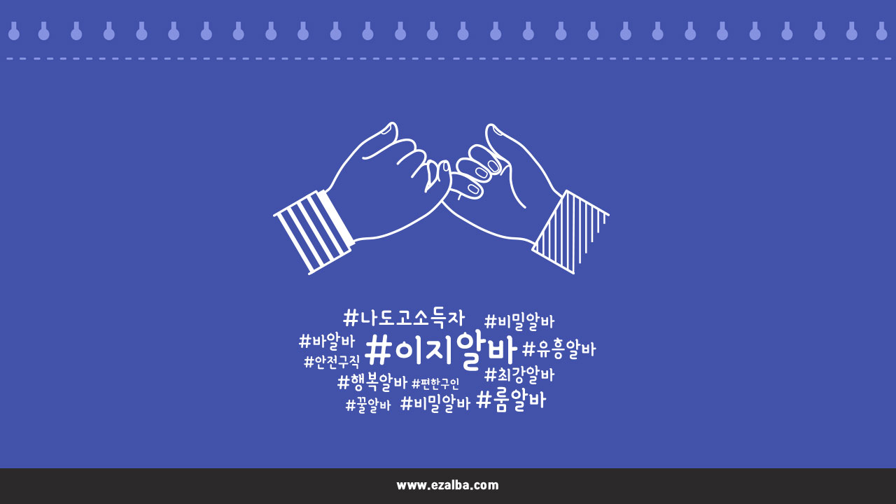
룸알바는 빠르게 변화하는 일자리 시장에서 중요한 부분을 차지합니다. 이 글에서는 룸알바의 급여, 취업, 면접 및 일자리 안내에 대해 자세히 알아보겠습니다. 업체 소개 및 업체 목록 지역별로 다양한 룸알바 업체가 있습니다. 업종별로 분류된 이지알바 업체 목록을 통해 여러분에게 가장 적합한 곳을 찾아보세요. 룸알바에서 일하기 위한 첫 단계는 무엇일까요? 바로 면접입니다. 면접...

로또에 당첨되는 꿈, 우리 모두 한 번쯤 꾸어보지 않았나요? 이제 그 꿈을 현실로 만들어줄 무료 로또번호 생성 서비스, 프리또를 소개합니다! 로또 645의 비밀: 확률과 통계의 마법 로또 645는 무작위 추첨으로 당첨 번호를 결정합니다. 하지만 빅데이터와 AI를 활용한 분석을 통해, 당첨 가능성을 극대화하는 번호 조합을 찾을 수 있습니다. 매주 업데이트되는 당첨번호...
카지노사이트의 인기 요인 최근 빅데이터 분석 결과에 따르면 카지노사이트의 인기는 다양한 게임 제공과 사용자 편의성 향상에서 기인합니다. 이용자들은 다양한 게임 옵션과 더불어, 편리한 접근성을 가장 중요하게 생각하는 경향이 있습니다. 카지노사이트 순위 및 추천 시스템 카지노친구는 사용자 리뷰와 전문가의 평가를 기반으로 한 순위 및 추천 시스템을 제공합니다. 고객 만족도가 높은 사이트를...